Datasheet4U Logo Datasheet4U.com

FCD380N60E - N-Channel MOSFET

General Description

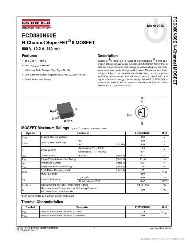
® ® SuperFET II MOSFET is Fairchild Semiconductor ’s first generation of high voltage super-junction (SJ) MOSFET family that is utilizing charge balance technology for outstanding low on-resistance and lower gate charge performance.This advanced technology is tailored to minimize conduction loss, provide superior switching performance, and withstand extreme dv/dt rate and higher avalanche energy.

Consequently, SuperFETII MOSFET is suitable for various AC/DC power conversion for system miniaturization and higher efficiency.

D G S D G D-PAK S MOSFET Maximum Ratings TC = 25oC unless otherwise noted Symbol VDSS VGSS ID IDM EAS IAR EAR dv/dt PD TJ, TSTG TL Parameter Drain to Source Voltage Gate to Source Voltage Drain Current Drain Current Single Pulsed Avalanche Energy Avalanche Current Repetitive Avalanche Energy Peak Diode Recovery dv/dt MOSFET dv/dt Power Dissipation (TC = 25oC) - Derate above 25oC - DC - AC -Continuous (TC = 25oC) -Continuous (TC = 100oC) - Pulsed (Note 1) (Note 2) (Note 1) (Note 1) (Note 3) (f > 1 Hz) FCD380N60E 600 ±20 ±30 10.2 6.4 30.6 211.6 2.3 1.06 20 100 106 0.85 -55 to +150 300 Unit V V V A A mJ A mJ V/ns W W/oC o o Operating and Storage Temperature Range Maximum Lead Temperature for Soldering Purpose, 1/8” from Case for 5 Seconds C C *Drain current limited by maximum junction temperature Thermal Characteristics Symbol RθJC RθJA Parameter Thermal Resistance, Junction to Case Thermal Resistance, Junction to Ambient FCD380N60E 1.18 100 Unit oC/W ©2012 Fairchild Semiconductor Corporation FCD380N60E Rev.

Overview

FCD380N60E N-Channel MOSFET March 2013 FCD380N60E N-Channel SuperFET® II MOSFET 600 V, 10.

Key Features

  • 650 V @TJ = 150°C.
  • Max. RDS(on) = 380 mΩ.
  • Ultra Low Gate Charge (Typ. Qg = 34 nC).
  • Low Effective Output Capacitance (Typ. Coss. eff = 97 pF).
  • 100% Avalanche Tested.